
 KTAR News 92.3
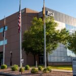
Applied Materials Inc. and Arizona State University on Thursday opened a $270 million research, development and prototyping facility to support the Valley’s growing semiconductor ecosystem.
The Materials-to-Fab Center consists of 50,000 square feet of cleanroom space and 20,000 square feet of wet and dry labs in the university’s MacroTechnology Works building at ASU Research Park. The facility is designed to foster innovations from ideation to fab prototype by leveraging Applied Materials’ semiconductor manufacturing equipment in a collaborative environment for academia, researchers and industry partners.
The collaboration of ASU’s engineering teams, Applied Materials technologists and industry partners will boost development of new chip technologies crucial to U.S. leadership in AI and

 Mediaite
 America News
 ABC30 Fresno World
 SOFREP
 ABC30 Fresno Sports
 NBC News
 The Fashion Spot
 The List
 RadarOnline